Currently the AET or other electron tomography method on material science samples are based on ADF-STEM images. Although currently it’s working well, there is some potential problems such as the high dose of ADF-STEM images could damage the sample during the tilt series acquisition which makes the reconstruction quality not good.And also, the STEM images cannot visualize low-atomic number elements such as carbon and oxygen, especially with the coalescence of high Z elements.
So, a better method needs to be applied into electron tomography whichis able to visualize low Z elements and requires lower dose. Recent advances in high-speed pixelated electron detectors have substantially facilitated the implementation of four-dimensional scanning transmission electron microscopy (4D-STEM). It records a full image of the STEM probe for many probe positions to visualize low-Z element with better quality and lower dose.
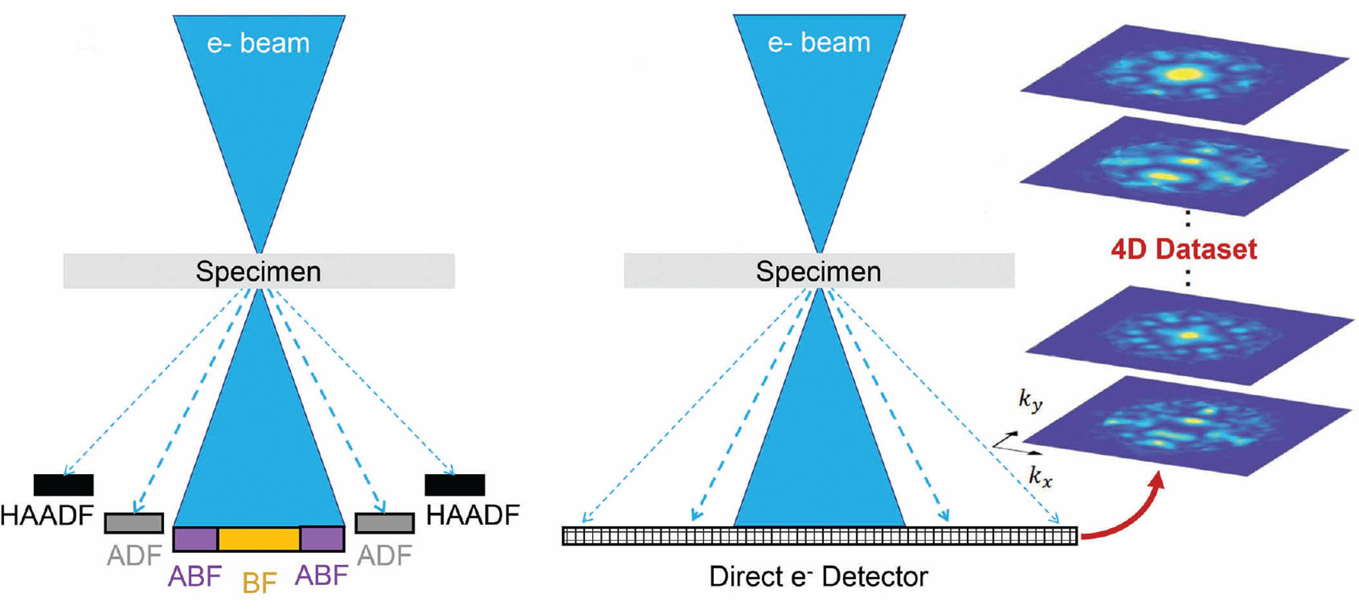
The principle of 4D-STEM (credit: Colin Ophus)
Here is an illustration of comparison between conventional STEM and 4D-STEM. The left handside is conventional STEM setting, we apply convergence beam in STEM mode, for each scanned position, usually we use some point detector like bright field detector or annular dark field detector. And the detectors just give one value related to the total dose the detector collected. For the High angle annular dark field detector, because these high angle scattered electron only represent a very small fraction of the total dose, like less than 5%, which is a big waste of electron doses. Now with the development of the direct pixelated detectors, we can record the diffraction pattern of each scan probe position like the right handside figure shows. That is why it’s called 4D-STEM, it means a 2D images of a converged electron probe, over a 2D grid of probe position, the 4D here means the x,y and diffraction pattern for each pixel (px and py).

The Comparison between tranditional STEM and 4D-STEM
With such kind of diffraction array, we can get much more information than the conventional STEM images with even smaller dose. A critical application of 4D-STEM is electron ptychography, which reveals the atomic structure of a specimen by reconstructing its transmission function from redundant convergent-beam electron diffraction patterns. With the method we can even recover the atomic potential for the sample and also the probe information.
Although 4D-STEM ptychography offers many advantages over conventional imaging modes, this emerging technique has not been fully applied to materials highly sensitive to electron beams. Our lab will focus on the potential advantages and its feasibility of 4D-STEM and techniques such as electron ptychography, which will be a game-changer for imaging extremely sensitive materials, such as metal−organic frameworks, hybrid halide perovskites, and supramolecular crystals.